
Mohit's Life and Career
Mohit in Childhood
I was born in Faridabad (part of Delhi NCR) on Nov 24, 1978. My dad worked as a teacher in one of the top schools in Delhi and used to accompany myself and my younger sister to school. We used to travel in local train, commuting a distance of 30km between home and school in Delhi; switching trains, buses and rickshaws and used to take around 3 hours (back and forth). As a kid, my journey to school was full of excitement to watch people selling stuff on railway station and other places anything from Chocolates to Comic books. However the commute time pushed us to relocate to Delhi in 1986. I did my schooling, graduation, trainings, jobs all in and around Delhi.
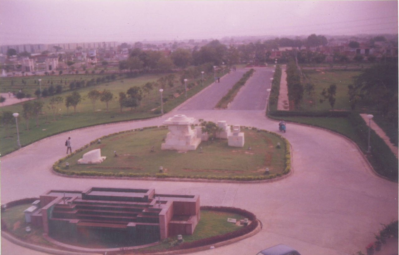
NSIT Campus in Year 1999
I must say I was an average student till class 10th until I become much more interested in Science & Technology. I was pretty good in Physics, Chemistry and Mathematics and was interested in becoming a doctor even though I never liked Biology to that extent. I was pretty confident that my pathetic hand-writing matched those of the doctors by the way they write on medical prescriptions. Jokes apart, despite of securing competitive marks in Physics and Chemistry in common entrance exams (i.e. Delhi PMT), I could not make it to the list due to not so good scores in Biology which kept me away from Medical industry, thus saving Mankind. However not to miss the chance, I did applied in couple of Engineering College entrance exams including Delhi College of Engineering (DCE), under Delhi University. Securing a ranking in top 200, I was able to get my desired stream – “Electronics and Communication Engineering” in Netaji Subhas Institute of Technology (NSIT, formerly Delhi Institute of Technology). This was a pretty proud moment as I was the only one from my school batch who could make it through to NSIT. NSIT is now an autonomous institution under the Government of Delhi and has consistently been in list of top 10 engineering colleges of India.
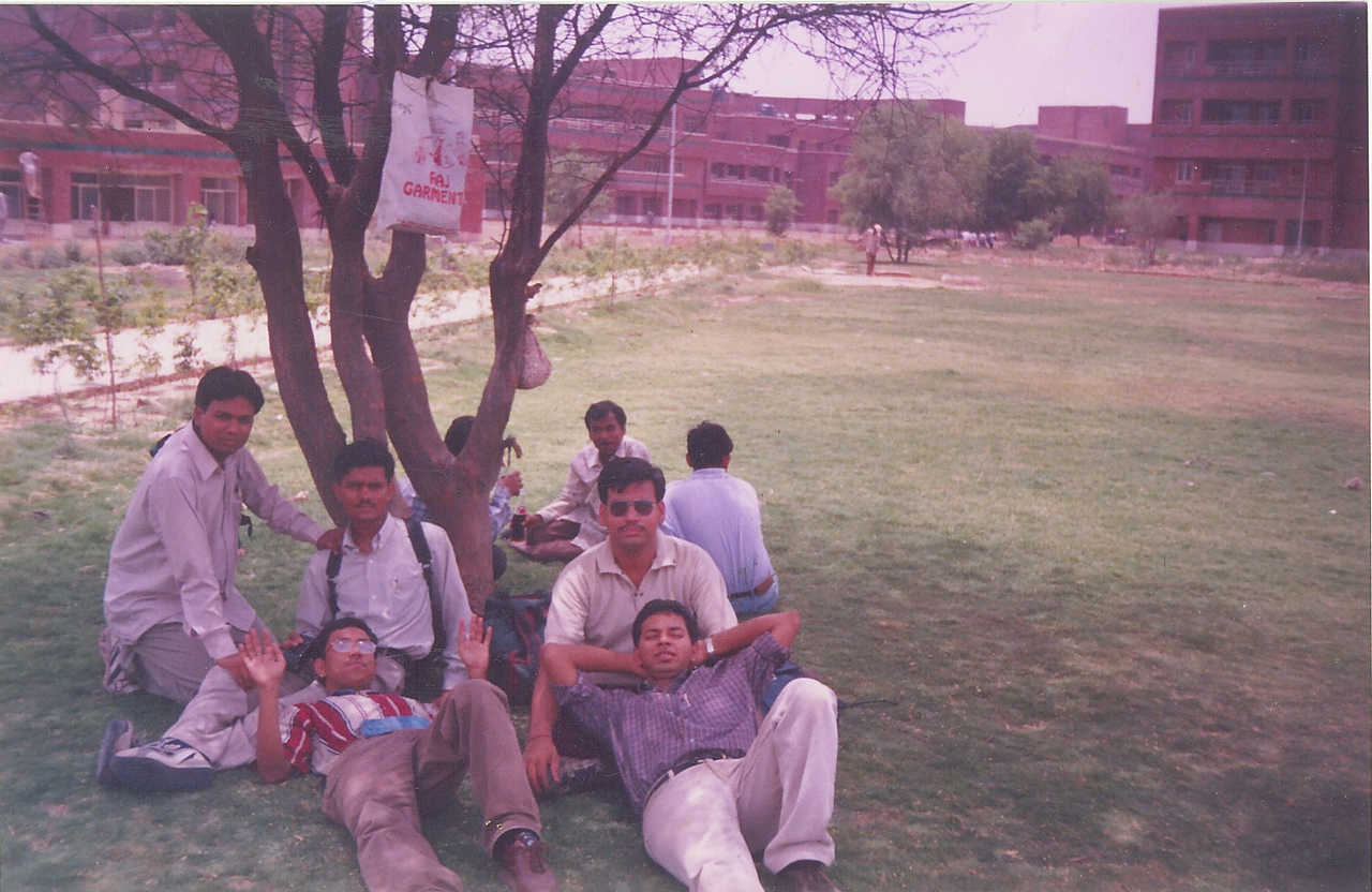
Aspiring Engineers (Batch :1996) just after one of the campus placement rounds
My time in college was the best ever with big change in culture (as compared to School for obvious reasons) and no dress code. First year was best spent in Kashmere gate, located in Central Delhi that was center of attraction for lot of tourists (being in old Delhi) and mouth watering street food before campus got moved to Dwarka, West Delhi. Though I was inclined towards getting into a core software firm and was not really interested in semiconductors, I still got selected in DCM Technologies as part of campus placement which was into chip design and design services. The company also offered two months internship in the pre-final semester (in 1999) where I created a Perl script that takes in VHDL/Verilog modules files and automatically creates top level file stitching them all together. Nowadays this is pretty standard offering from EDA tool vendors. Industrial training also changed my perception that chip design is not just about electrons flowing from source to drain but practical aspects in the application widely differ that made me eager to learn more.

The “Pebbles” Team.
I joined DCM Technologies later in June 2000 after completing my graduation. I was assigned on project “Pebbles” – test card used to stress Serial ATA bus and provide hooks for debugging Serial ATA interfaces in a test system environment. I was responsible for the design of complete Link Layer and PHY interface for the 1st generation Serial ATA(1.5Gbps). This was done for Intel and around the time when Serial ATA Specifications were being developed by Intel (in year 2000). Later I worked on InfiniBand and PCI-Express (Gen-I) projects, owning complete link layer design for the protocol stack all the way from specifications till RTL design before both these protocols got married together around 2004. With no to little information available at that time over Internet (don’t recall if Google was available or popular that time), it was pretty exciting to work directly on these cutting edge technologies that today form the base of high performance computing and networking. Being a small company with not many managers per project unlike big MNCs, put good amount of responsibility on engineers. For instance, the design team for most of these projects was no big than 3-4 engineers along with one project manager, so all the decisions were taken within the team. DCM Technologies also laid a very strong foundation of design/RTL as this was the main focus for the whole company (being a fabless company). Being a design services and CMM-level 5 company, there was a lot of focus on documentation. I recall that we had a quality VP that used to review the design all the time to check if micro-architecture document matches the RTL code and vice versa. However this laid a very strong foundation on both design documentation as well as RTL coding.
Fun at Work(DCM). Can’t believe everyone except one is now in Freescale!!
During my tenure in DCM, I got the “Best Engineer Merit Award” for year 2001 on the basis of voting by engineering committee, rather than being nominated by manager.
In early 2002, I presented my first set of papers on “Handling Multiple Clocks in Design” and “Design Tips/Tricks for FPGA/ASIC” in Synopsys SNUG, Bangalore.
Testing USB PHY in ST Micro “Crolles” Lab in France
Wanting to grow my learning beyond RTL design concepts, I moved to ST Microelectronics in Central Research and Development (CR&D) Dept. in 2002. This was an interesting change that made me realize RTL is not end of the world when it cames to chip-design. I was responsible for the design of Hi-Speed USB2.0 Host PHY. Though Transceiver (Analog) was designed by a team in Grenoble, France, I was assigned to leverage the existing USB Device and make necessary changes to add Host mode with an evolving and changing UTMI+ interface. Though the initial Device PHY was in 0.18um technology, there were significant changes to the architecture to add Host mode along with a technology migration from 0.18um to 0.13 um, that also had a significant impact on Digital. Around the same time I went to ST Microelectronics Crolles/Grenoble (in France) for two weeks to support some of the validation work along with a short trip to Castellato, Italy to test PHY on tester. During the course, I also got responsibility as a project leader for the complete USB Subsystem in 90nm that includes the USB PHY, Host Controller and arrays of wrapper to covert the third party controller interface from AHB to propriety ST Bus interconnect. Subsystem was being done for ST Setup box, DVD and imaging group that includes some of the clients like HP. In 2004, our small team of USB design was awarded CEO “Best Team Bronze Award” at global level as USB implementation was one of the big roadblocks and important module for several ST products around that time and it was not easy to get certification (to allow OEMs to stamp USB Hi-Speed Logo on their products) from third party company in Belgium.
Later in (2004), I moved to Agilent Technologies, a fabless company and was responsible for USB and SDIO module for HP Multi Function Printers (Agilent being spin off from HP, majority of the business still included work for HP). I also got rated as “Best Engineer” in Agilent, India by US team who directly worked with the initial batch that was hired. Other work included designing of the JBIG encryption blocks for one of the MFP projects before I left Agilent and joined Freescale.
Freescale Technology Forum @ 2010 , Bangalore
I joined Freescale (in 2005) as a Design Lead and Systems Architect in Microcontroller Solutions Group (MSG) and was responsible for complete SoC architecture along with leading the SoC design for couple of projects. This is also the time when I got married (of course that was not the motivation to change the company and was a just a co-incidence). Along with SoC Design, I also led the design for couple of IP projects within MSG. During the course, I also supported the group to setup a small post silicon validation lab and evaluated equipments (Logic Analyzers, Oscilloscopes, Pattern generators etc) to be purchased in order to validate design for next several years.
I moved to Systems Engineering in 2008 , with my main responsibilities that included product definition and writing specifications for MCU/MPU based products for Mid-high end Consumer and Industrial market. During this course, i got opportunity to travel across the world , meeting more than 50 customers worldwide. Energy Metering, Metrology and Embedded Security had been some of the areas i was highly focussed on. I also led the Security Asset team across Microcontroller and Automotive Business group until early 2015. Since my work involves lot of research, it gives me good opportunity to write technical papers, articles, participate in various conferences and share practical experiences. During this journey I got lot of positive feedback on my publications. Readers have often asked me forcing me to think if I should write a book compiling all the practical experiences. It took me almost 4 years to complete the book “The Art of Hardware Architecture: Design Methods and Techniques for Digital circuits” that includes all customer diagrams and focused on Practical aspects of chip design. First revision of the book came up through Springer in late 2013.
I do enjoy writing articles whenever I get time. Till date I have more than 50 publications, lately most focused on Metering and embedded security. Once can find all the articles in the Articles section of this website. I have been invited blogger on eetimes (Blog : Beyond Bits and Bytes), through have not been very active. Currently i am working on another book on "Embedded System Design” with the first revision focussed on SoC architecture, due for May 2016 release.
Award for “Master Author” in Freescale(2010)
Being in systems definition, I get lot of opportunities to travel all around the world for all sort of customer meetings and definition summits. So far I have visited more than 50 customers around the world. This has given me excellent experience to know practical aspects on how customers see things differently that is not so obvious when we design ASICs.
On Daughter’s 1st Birthday(2010)
I did relocated to Freescale, Austin in 2013, through this was a major move for my family. At home and over weekends, majority of the time is best spent with family, social activities and playing with my daughters. When I’m not on the computer (which is usually not the case), I most often spend my free time reading about Spirituality, Mind over Matter, Energy meditation and hitting the fitness center/Gym. More recently I been more focussed on health for obvious reasons :-). I love adventure sports of any nature but over past couple of years, have not really got an opportunity (which is obvious after marriage and kids). That’s me.
– Mohit Arora
February , 2016